Implementation of 20 nm Graphene Channel Field Effect Transistors Using Silvaco TCAD Tool to Improve Short Channel Effects over Conventional MOSFETs
DOI:
https://doi.org/10.46604/aiti.2021.8098Keywords:
graphene, MOSFET, Silvaco TCAD, graphene FET, 2D low power design, 2D-materialAbstract
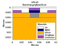
In recent years, demands for high speed and low power circuits have been raised. As conventional metal oxide semiconductor field effect transistors (MOSFETs) are unable to satisfy the demands due to short channel effects, the purpose of the study is to design an alternative of MOSFETs. Graphene FETs are one of the alternatives of MOSFETs due to the excellent properties of graphene material. In this work, a user-defined graphene material is defined, and a graphene channel FET is implemented using the Silvaco technology computer-aided design (TCAD) tool at 100 nm and scaled to 20 nm channel length. A silicon channel MOSFET is also implemented to compare the performance. The results show the improvement in subthreshold slope (SS) = 114 mV/dec, ION/IOFF ratio = 14379, and drain induced barrier lowering (DIBL) = 123 mV/V. It is concluded that graphene FETs are suitable candidates for low power applications.
References
The International Technology Roadmap for Semiconductors, “International Technology Roadmap for Semiconductors 2.0, 2015 Edition, Beyond C-MOS,” https://www.semiconductors.org/wp-content/uploads/2018/06/6_2015-ITRS-2.0-Beyond-CMOS.pdf, 2015.
V. Tayade and S. Lanudkar, “A Review of Emerging Devices Beyond MOSFET for High Performance Computing,” International Conference on Emerging Smart Computing and Informatics, pp. 34-38, March 2020.
I. Meric, C. R. Dean, N. Petrone, L. Wang, J. Hone, P. Kim, et al., “Graphene Field-Effect Transistors Based on Boron-Nitride Dielectrics,” Proceedings of the IEEE, vol. 101, no. 7, pp. 1609-1619, July 2013.
K. S. Novoselov, A. K. Geim, S. V. Morozov, D. E. Jiang, Y. Zhang, S. V. Dubonos, et al., “Electric Field Effect in Atomically Thin Carbon Films,” Science, vol. 306, no. 5696, pp. 666-669, October 2004.
F. Schwierz, “Graphene Transistors: Status, Prospects, and Problems,” Proceedings of the IEEE, vol. 101, no. 7, pp. 1567-1584, July 2013.
J. M. Marmolejo-Tejada and J. Velasco-Medina, “Review on Graphene Nanoribbon Devices for Logic Applications,” Microelectronics Journal, vol. 48, pp. 18-38, February 2016.
Y. Y. Chen, A. Sangai, A. Rogachev, M. Gholipour, G. Iannaccone, G. Fiori, et al., “A SPICE-Compatible Model of MOS-Type Graphene Nano-Ribbon Field-Effect Transistors Enabling Gate- and Circuit-Level Delay and Power Analysis under Process Variation,” IEEE Transactionsons on Nanotechnology, vol. 14, no. 6, pp. 1068-1082, November 2015.
F. W. Chen, H. Ilatikhameneh, G. Klimeck, Z. Chen, and R. Rahman, “Configurable Electrostatically Doped High-Performance Bilayer Graphene Tunnel FET,” IEEE Journal of Electron Devices Society, vol. 4, no. 3, pp. 124-128, May 2016.
T. K. Agarwal, A. Nourbakhsh, P. Raghavan, I. Radu, S. De Gendt, M. Heyns, et al., “Bilayer Graphene Tunneling FET for Sub-0.2 V Digital CMOS Logic Applications,” IEEE Electron Device Letters, vol. 35, no. 12, pp. 1308-1310, December 2014.
Y. Lv, W. Qin, Q. Huang, S. Chang, H. Wang, and J. He, “Graphene Nanoribbon Tunnel Field-Effect Transistor via Segmented Edge Saturation,” IEEE Transactions on Electron Devices, vol. 64, no. 6, pp. 2694-2701, June 2017.
A. Rassekh and M. Fathipour, “A Single-Gate SOI Nanosheet Junctionless Transistor at 10-nm Gate Length: Design Guidelines and Comparison with the Conventional SOI FinFET,” Journal of Computational Electronics, vol. 19, no. 2, pp. 631-639, June 2020.
N. E. I. Boukortt, B. Hadri, A. Caddemi, G. Crupi, and S. Patanè, “3-D Simulation of Nanoscale SOI n-FinFET at a Gate Length of 8 nm Using ATLAS SILVACO,” Transactions on Electrical and Electronic Materials, vol. 16, no. 3, pp. 156-161, 2015.
J. C. Pravin, D. Nirmal, P. Prajoon, and J. Ajayan, “Implementation of Nanoscale Circuits Using Dual Metal Gate Engineered Nanowire MOSFET with High-k Dielectrics for Low Power Applications,” Physica E: Low-Dimensional Systems and Nanostructures, vol. 83, pp. 95-100, September 2016.
J. Ning, Y. Wang, X. Feng, B. Wang, J. Dong, D. Wang, et al., “Flexible Field-Effect Transistors with a High On/Off Current Ratio Based on Large-Area Single-Crystal Graphene,” Carbon, vol. 163, pp. 417-424, August 2020.
Z. He, C. Yu, Q. Liu, X. Song, X. Gao, J. Guo, et al., “High Temperature RF Performances of Epitaxial Bilayer Graphene Field-Effect Transistors on SiC Substrate,” Carbon, vol. 164, pp. 435-441, August 2020.
K. Tamersit and F. Djeffal, “Boosting the Performance of a Nanoscale Graphene Nanoribbon Field-Effect Transistor Using Graded Gate Engineering,” Journal of Computational Electronics, vol. 17, no. 3, pp. 1276-1284, September 2018.
K. Tamersit, “A Computational Study of Short-Channel Effects in Double-Gate Junctionless Graphene Nanoribbon Field-Effect Transistors,” Journal of Computational Electronics, vol. 18, no. 4, pp. 1214-1221, December 2019.
T. Radsar, H. Khalesi, and V. Ghods, “Improving the Performance of Graphene Nanoribbon Field-Effect Transistors by Using Lanthanum Aluminate as the Gate Dielectric,” Journal of Computational Electronics, vol. 19, no. 4, pp. 1507-1515, December 2020.
M. S. Fahad, A. Srivastava, A. K. Sharma, and C. Mayberry, “Analytical Current Transport Modeling of Graphene Nanoribbon Tunnel Field-Effect Transistors for Digital Circuit Design,” IEEE Transactions on Nanotechnology, vol. 15, no. 1, pp. 39-50, January 2016.
F. Djeffal, T. Bentrcia, M. A. Abdi, and T. Bendib, “Drain Current Model for Undoped Gate Stack Double Gate (GSDG) MOSFETs Including the Hot-Carrier Degradation Effects,” Microelectronics Reliability, vol. 51, no. 3, pp. 550-555, March 2011.
M. A. Abdi, F. Djeffal, Z. Dibi, and D. Arar, “A Two-Dimensional Analytical Subthreshold Behavior Analysis Including Hot-Carrier Effect for Nanoscale Gate Stack Gate All Around (GASGAA) MOSFETs,” Journal of Computational Electronics, vol. 10, no. 1-2, pp. 179-185, June 2011.
X. Ma, W. Gu, J. Shen, and Y. Tang, “Investigation of Electronic Properties of Graphene/Si Field-Effect Transistor,” Nanoscale Research Letters, vol. 7, no. 1, 677, December 2012.
M. S. Mobarakeh, N. Moezi, M. Vali, and D. Dideban, “A Novel Graphene Tunneling Field Effect Transistor (GTFET) Using Bandgap Engineering,” Superlattices and Microstructures, vol. 100, pp. 1221-1229, December 2016.
Y. Kuang, Y. Liu, Y. Ma, J. Xu, X. Yang, X. Hong, et al., “Modeling and Design of Graphene GaAs Junction Solar Cell,” Advances in Condensed Matter of Physics, vol. 2015, 326384, 2015.
SILVACO International, “ATLAS User’s Manual, Device Simulation Software, Volume I,” http://statistics.roma2.infn.it/~messi/SIC/sic_21-01-04/atlas98-v1_users.pdf, November 1998.
O. Weber, “FDSOI vs FinFET: Differentiating Device Features for Ultra Low Power & IoT Applications,” IEEE International Conference on IC Design and Technology, pp. 1-3, May 2017.
M. Y. Han, B. Özyilmaz, Y. Zhang, and P. Kim, “Energy Band-Gap Engineering of Graphene Nanoribbons,” Physical Review Letter, vol. 98, no. 20, 206805, May 2007.
Z. Chen, Y. M. Lin, M. J. Rooks, and P. Avouris, “Graphene Nano-Ribbon Electronics,” Physica E: Low-Dimensional Systems and Nanostructures, vol. 40, no. 2, pp. 228-232, December 2007.

Published
How to Cite
Issue
Section
License
Submission of a manuscript implies: that the work described has not been published before that it is not under consideration for publication elsewhere; that if and when the manuscript is accepted for publication. Authors can retain copyright in their articles with no restrictions. is accepted for publication. Authors can retain copyright of their article with no restrictions.
Since Jan. 01, 2019, AITI will publish new articles with Creative Commons Attribution Non-Commercial License, under The Creative Commons Attribution Non-Commercial 4.0 International (CC BY-NC 4.0) License.
The Creative Commons Attribution Non-Commercial (CC-BY-NC) License permits use, distribution and reproduction in any medium, provided the original work is properly cited and is not used for commercial purposes.


