A Study on Aluminum Pad Large Deformation during Copper Wirebonding for High Power IC Package
Keywords:
copper wirebonding, large plastic deformation, impact-contact, hourglass defectAbstract
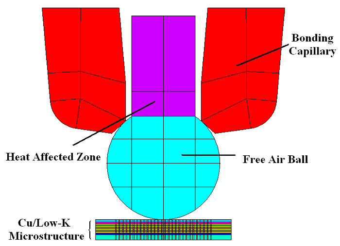
In this paper, a 3-D finite element prediction on aluminum pad squeeze during copper wirebonding process for high power IC package is presented. ANSYS Parametric Design Language (APDL) has been implemented on modelling, mesh density, boundary condition (BC), impact stage and contact mode for first bond process. The ANSYS/LS-DYNA solver is applied to solve dynamics and LS-PREPOST is used to observe the predicted large plastic deformation on bond pad and stress on microstructure under pad. In view of high power IC package, larger diameter of copper wire is required for electric loading for its low cost. In this research, a large diameter of 2 mil (50 um) uncoated pure copper (4N) wire is applied to simulate first bond impact-contact process. As the scale double enlarged, the problems encountered in simulation are usually evident. Preliminary results on impact stage demonstrate that negative volume/hourglass on large distortion can be solved by tune-up inertial contact settings and mesh density. However, sever hourglass defect would occur on ultrasonic stage and remain a pending problem. A series of prediction has been conducted on first bond process during impact stage and the results can then be applied to the dynamic wirebonding assembly process.
References
Y. J. Lin, C. Kang, L. Chua, W. K. Choi, and S. W. Yoon, “Advanced 3D eWLB-PoP (embedded wafer level ball grid array-package on package) technology,” Proc. 66th Electronic Components and Technology Conference, May. 2016, pp. 1772-1777.
M. C. Hsieh, K. T. Kang, H. C. Choi, and Y. C. Kim, “Thin profile flip chip package-on-package development,” Proc. 11th International Microsystems, Packaging, Assembly and Circuits Technology Conference, Oct. 2016, pp. 143-147.
N. Srikanth, S. Murali, Y. M. Wong, and C. J. Vath III, “Critical study of thermosonic copper ball bonding,” Thin Solid Films, vol. 462, pp.339-345, 2004.
D. S. Liu, Y. C. Chao, and C. H. Wang, “Study of wire bonding looping formation in the electric packaging process using the three-dimensional finite element method,” Finite Element in Analysis and Design, vol. 40, no. 3, pp. 263-286, 2004.
Y. Liu, S. Irving, and T. Luk, “Thermosonic wire bonding process simulation and bond pad over active stress analysis,” IEEE Transactions on Electronics Packaging Manufacturing, vol. 31, no. 1, pp. 61-71, 2008.
F. Y. Hung, T. S. Lui, L. H. Chen, and Y. T. Wang, “Recrystallization and fracture characteristics of thin copper wire,” Journal of Materials Science, vol. 42, no. 14, pp. 5476-5482, 2007.
C. Hanga, C. Wang, M. Shi, X. Wu, and H. Wang, “Study of copper free air ball in thermosonic copper ball bonding,” Proc. 6th International Electric Packaging Technology Conference, Aug. - Sep., 2005, pp. 414-418.
W. Y. Chang, H. C. Hsu, S. L. Fu, Y. S. Lai, and C. L. Yeh, “An investigation on heat affected zone for Au wire/Cu wire and advanced finite element wirebonding model,” Proc. 3rd Microsystems, Packaging, Assembly & Circuits Technology Conference, Oct. 2008, pp. 419-423.
C. L. Yeh, Y. S. Lai, and C. L. Kao, “Transient simulation of wire pull test on Cu/low-K wafers,” IEEE Transactions on Advanced Packaging, vol. 29, no. 3, pp. 631-638, 2006.
H. C. Hsu, C. Y. Hu, W. Y. Chang, C. L. Yeh, and Y. S. Lai, “Dynamic finite element analysis on underlay microstructure of Cu/low-k wafer during wirebonding,” Finite Element Analysis, pp. 453-478, 2010.
S. K. Prasad, Advanced wirebond interconnection technology, Kluwer Academic Publishers, pp. 3-55, 2004.
R. C. J. Wang, C. C. Lee, L. D. Chen, K. Wu, and K. S. Chang-Liao, “A study of Cu/Low-k stress-induced voiding at via bottom and its microstructure effect,” Microelectronic Reliability, vol. 46, no. 9, pp.1673-1678, 2006.
Published
How to Cite
Issue
Section
License
Submission of a manuscript implies: that the work described has not been published before that it is not under consideration for publication elsewhere; that if and when the manuscript is accepted for publication. Authors can retain copyright in their articles with no restrictions. is accepted for publication. Authors can retain copyright of their article with no restrictions.

Since Jan. 01, 2019, AITI will publish new articles with Creative Commons Attribution Non-Commercial License, under The Creative Commons Attribution Non-Commercial 4.0 International (CC BY-NC 4.0) License.
The Creative Commons Attribution Non-Commercial (CC-BY-NC) License permits use, distribution and reproduction in any medium, provided the original work is properly cited and is not used for commercial purposes.